Home /Tool Processing Services /

Durable Prototype Circuit Board Assembly , Flexible Pcb Board Nickel Palladium Surface

Durable Prototype Circuit Board Assembly , Flexible Pcb Board Nickel Palladium Surface

Brand Name:China chao sheng
Certification:ISO/UL/RoHS/TS
Model Number:CSPCB1343
Minimum Order Quantity:1PCS
Delivery Time:18-20day
Payment Terms:T/T, Western Union
Contact Now

Add to Cart

Active Member
Location: Hong kong Hong kong China
Address: Huishang Building, 19-128 Nathan Road, Yau Tsim Sha Tsui, Yau Tsim, Hong Kong
Supplier`s last login times: within 48 hours
Shipping
lt's easy to get a shipping quote! Just click the button below and complete the short form.
Get Shipping Quote
Product Details Company Profile
Product Details

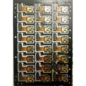
6Layers 2nd order HDI Rigid Flex PCB FR4 / Polyimide Material ENIG Hasl OSP Surface Finish,rigid flex circuit boards,rigid flexpcb

Product Type: High Pixel Camera

Size: 12*6.80mm/1PCS

Productstructure: FR-4+TG170+Panasonic PI, four layers of soft shadow combination, minimum hole 0.15mm, plate thickness 1.60mm, nickel palladium gold 3U",

Printed circuit board (pcb) and PCBA products
Communication terminal, communication station, electronic communication, optical fiber, optical module, communication equipment, communication instrument, computer, household appliance, testing equipment, testing instrument, instrument, SD card, SG card, mobile phone, computer, various antennas, cars, music Equipment, playback equipment, banking equipment, medical instruments, medical equipment, medical equipment, aerospace, aviation, military, LED, OLED, OLCD power control power supply, industrial power supply, communication power supply, automotive power supply, office equipment, digital products,computers,etc.Applications;
Flexible circuit board (FPC) and FPCA product areas
CD, hard disk, printer, fax machine, scanner, sensor, mobile phone, connector, module, walkie-talkie antenna card, high-end camera, digital camera, laser head, CD, medical, instrumentation, drive, automotive instrumentation, medical instrument, Medical equipment, banking equipment, industrial instruments, LED light bars, military, aviation, aerospace, defense and other high-tech products, of which more than 70% of the products are exported to Europe, America, Europe, Central Europe, Western Europe, Southeast Asia, Asia-Pacific and other countries and area.

Our Services

We are a Manufacturer & Supplier Specializing in Double Side PCB, Multi-Layer PCB, F4BK PCB, Ceramic PCB, Rogers PCB, Aluminum PCB. Meanwhile, we provide PCBA ( Assembly) and ODM, OEM service. We are specializes in a full SMT and through hole PCBA assembly, obtaining components, building prototype quantities, and testing. High quality,good price and service.

  1. Delivery time:5-7days.
  2. Certificates:UL,ISO9001,RoHS

Our capability

  1. Our professional engineering team can put your project into production in a short time. Sample pictures and BOM are needed to make customized products
  2. We can supply CAD and Pro-E designed precision moulds. Moulds can be designed and manufactured according to customers' requests or samples. Plastic injection processing available.
  3. We have advanced equipment for through-hole and SMT DIP COB cable assembly.
  4. ROHS compliant and lead-free process.
  5. In-circuit, functional tests& burn-in tests, full system test
  6. High output to guarantee prompt delivery.

PCB, FPC product application field

Various digital products, automotive new energy, automotive products, military, aerospace, medical, wireless terminals, wired terminals, communication equipment, communication stations, finance, industrial industrial control, consumer electronics, educational equipment, smart devices, smart products, security, LED, computer, mobile phone and other electronic products

Detailed Specification of Flexible PCB Manufacturing

Technical Specification
Layers:4~30 Layers(flex Pcb) and 4~80 (rigid flex) 
Min Panel Size:5mm x 8mm 
Max Panel Size:250 x 520mm 
Min Finished board thickness:0.05mm (1 sided inclusive copper) 
Max Finished board thickness:0.3mm (2 sided inclusive copper) 
Finished board thickness tolerance:±0.02~0.03mm 
Material:Kapton, Polyimide, PET 
Base copper thickness (RA or ED):1/3 oz, 1/2 oz, 1oz, 2oz 
Base PI thickness:0.5mil, 0.7mil, 0.8mil, 1mil, 2mil 
Stiffner:Polyimide, PET, FR4, SUS 
Min Finished hole diameter:Φ 0.15mm 
Max Finished hole diameter:Φ 6.30mm 
Finished hole diameter tolerance (PTH):±2 mil ( ±0.050mm) 
Finished hole diameter tolerance (NPTH):±1 mil ( ±0.025mm) 
Min width/spacing (1/3oz):0.05mm/0.06mm 
Min width/spacing (1/2oz):0.06mm/0.07mm 
Min width/spacing (1oz):Single layer: 0.07mm/0.08mm 
Double layer: 0.08mm/0.09mm 
Aspect Ratio6:018:01
Base Copper1/3Oz--2Oz3 Oz for Prototype
Size ToleranceConductor Width:±10%W ≤0.5mm
Hole Size: ±0.05mmH ≤1.5mm
Hole Registration: ±0.050mm 
Outline Tolerance:±0.075mmL ≤50mm
Surface TreatmentENIG: 0.025um - 3um 
OSP: 
Immersion Tin: 0.04-1.5um 
Dielectric StrengthAC500V 
Solder Float288℃/10sIPC Standard
Peeling Strength1.0kgf/cmIPC-TM-650
Flammability94V-OUL94


Quotation Requirement :
1) Following specifications are needed for quotation:
a) Base material
b) Board thickness:
c) Copper thickness
d) Surface treatment:
e) color of solder mask and silkscreen:
f) Quantity

Shiping method:
1) By DHL, Fedex, UPS, TNT etc.
2) By sea if it is possible
3) By air

Surface treatment:
full board OSP, full board immersion gold, whole board electric nickel gold, electric gold + immersion gold, electric gold + OSP, OSP + immersion gold, OSP + carbon bridge, gold finger, OSP + gold finger, immersion gold + gold finger, Shen tin, immersion silver, lead-free tin spray

FAQ:
Q: What files do you use in PCB fabrication?
A: Gerber or Eagle, BOM listing, X, Y sitting report, PNP and Components Position
Q: Is it possible you could offer sample?
A: Yes, we can custom you sample to test before mass production
Q: When will I get the quotation after sent Gerber, BOM and test procedure?
A: Within 6-48hours for PCB quotation and around 24-48 hours for PCBA quotation.
Q: According to the difficulty of high-layer boards, How can I know the process of my PCB production?
A: 7-35days for PCB production and components purchasing, and 14-20days for PCB assembly and Testing
Q: How can I make sure the quality of my PCB?
A: We ensure that each piece of PCB, PCBA products work well before shipping. We'll test all of them according to your test procedure.

PCB, FPC process production capability

Technical ltemMassProductAdvanced Technology
201620172018
Max.Layer Count26L36L80L
Through-hole plate2~45L2~60L2~80L
Max.PCBSize(in)24*52"25*62"25*78.75"
The layer number of FPC1~36L1~50L1~60L
Max.PCBSize(in)9.8"*196"9.8"*196"10"*196"Reel to reel
Layeredplatelayer2~12L2~18L2~26L
Max.PCBSize(in)9"*48"9"*52"9"*62"
Combination of hard and soft layers3~26L3~30L3~50L
Interconnect HDI5+X+5Interconnect HDI7+X+7Interconnect HDI8+X+8,Interconnect HDI
HDI PCB4~45L4~60L4~80L
Interconnect HDI3+20+34+X+4Interconnect HDI4+X+4,Interconnect HDI
Max.PCBSize(in)24"*43"24"*49"25"*52"
MaterialFR-4 RogersFR-4 RogersFR-4 Rogers
Base materialHalogenfree,LowDKHalogenfree,LowDKHalogenfree,LowDK
Build-up MaterialFR-4FR-4FR-4
BOard,Thickness(mm)Min.12L(mm)0.430.42~8.0mm0.38~10.0mm
Min.16L(mm)0.531.60~8.0mm0.45~10.0mm
Min.18L(mm)0.632.0~8.00.51~10.0mm
Min.52L(mm)0.82.50~8.0mm0.65~10.0mm
MAX(mm)3.510.0mm10.0mm
Min.CoreThickness um(mil)254"(10.0)254"(10.0)0.10~254(10.0mm)
Min.Build up Dielectric38(1.5)32(1.3)25(1.0)
BaseCopperWeightInner Layer4/1-8 OZ4/1-15 OZ4/1-0.30mm
Out Layer4/1-10 OZ4/1-15 OZ4/1-30 OZ
Gold thick1~40u"1~60u"1~120u"
Nithick76~127u"76~200u"1~250u"
Min.HOle/Land um(mil)150/300(6/12)100/200(4/8)100/200(4/8)
Min.Laser via/landum(mil)60/170(2.4/6.8)50/150(2/6)50/150(2/6)
Min. IVH,Hole size/landum(mil)150/300(6/12)100/200(4/8)100/200(4/8)
DieletricThickness38(1.5)32(1.3)32(1.3)
125(5)125(5)125(5)
SKipviaYesYesYes
viaoNhie(laserviaon BuriedPTH)YesYesYes
Laser Hole FillingYesYesYes
TechnicalltemMass ProductAdvanced Technolgy
2017year2018year2019year
Drill hole depth ratioThroughHole2017year.40:1.40:1
Aspet RatioMicro Via.35:11.2:11.2:1
Copper Filling Dimple Size um(Mil)10(0.4)10(0.4)10(0.4)
Min.LineWidth&spacelnner Layer um(mil)45/45(1.8/1.8)38/38(1.5/1.5)38/38(1.5/1.5)
Plated Layer um(mil)45/45(1.8/1.8)38/38(1.5/1.5)38/38(1.5/1.5)
BGAPitch mm(Mil)0.30.30.3
Min.PTH Hole ring um(mil)75(3mil)62.5(2.5mil)62.5(2.5mil)
Line Width Control∠2.5MIL±0.50±0.50±0.50
2.5Mil≤L/W∠4mil±0.50±0.50±0.50
≦3mil±0.60±0.60±0.60
Laminated structureLayer by layer3+N+34+N+45+N+5
Sequential Build-up20L Any Layer36L Any Layer52L Any Layer
Multi-layer overlayN+NN+NN+N
N+X+NN+X+NN+X+N
sequential Lamination2+(N+X+N)+22+(N+X+N)+22+(N+X+N)+2
Soft and hard bonding2+(N+X+N)+22+(N+X+N)+22+(N+X+N)+2
PTH filling processPTH resin plug hole + plating fill
Electroplated hole/copper plug hole
PTH resin plug hole + plating fill
Electroplated hole/copper plug hole
PTH resin plug hole + plating fill
Electroplated hole/copper plug hole
China Durable Prototype Circuit Board Assembly , Flexible Pcb Board Nickel Palladium Surface supplier

Durable Prototype Circuit Board Assembly , Flexible Pcb Board Nickel Palladium Surface

Inquiry Cart 0