OEM Multilayer PCB Board High Output Fast Prototyping For LED Driver Products
Brand Name:China chao sheng
Certification:ISO/UL/RoHS/TS
Model Number:three layers of iron-based pit PCB
Minimum Order Quantity:1PCS
Delivery Time:15-18day
Payment Terms:T/T, Western Union
Contact Now
Add to Cart
Active Member
Location:
Hong kong Hong kong China
Address:
Huishang Building, 19-128 Nathan Road, Yau Tsim Sha Tsui, Yau Tsim, Hong Kong
Supplier`s last login times:
within 48 hours
Shipping
lt's easy to get a shipping quote! Just click the button below and complete the short form.
Get Shipping Quote
Product Details
Company Profile
Product Details
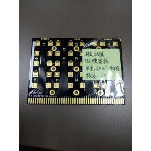
three layers of iron-based pit PCB LED driver products iron base pit PCB+FR-4+PPTG180, cop per thickness rigid flex pcb
Product Description
- Product area: LED driver products
- Number of layers: three layers of iron-based pit PCB
- Plate thickness: 2.0mm
- Product structure: iron base pit PCB+FR-4+PPTG180, copper thickness
- 5OZ, sinking hole, electric nickel gold 5U"
- Printed Circuit Boards are 94V0 compliant, and adhere to IPC610 Class 2 international PCB
- standard.
- Quantities range from prototype to volume production.
- 8. 100% E-Test
- Packaging: Vacuum Packaging + Moisture-proof Bead + Humidity Card + Carton
- Printed circuit board (pcb) and PCBA products
Communication terminal, communication station, electronic communication, optical fiber, optical module, communication equipment, communication instrument, computer, household appliance, testing equipment, testing instrument, instrument, SD card, SG card, mobile phone, computer, various antennas, cars, music Equipment, playback equipment, banking equipment, medical instruments, medical equipment, medical equipment, aerospace, aviation, military, LED, OLED, OLCD power control power supply, industrial power supply, communication power supply, automotive power supply, office equipment, digital products,computers,etc.Applications;
Flexible circuit board (FPC) and FPCA product areas
CD, hard disk, printer, fax machine, scanner, sensor, mobile phone, connector, module, walkie-talkie antenna card, high-end camera, digital camera, laser head, CD, medical, instrumentation, drive, automotive instrumentation, medical instrument, Medical equipment, banking equipment, industrial instruments, LED light bars, military, aviation, aerospace, defense and other high-tech products, of which more than 70% of the products are exported to Europe, America, Europe, Central Europe, Western Europe, Southeast Asia, Asia-Pacific and other countries and area.
PCB, FPC process production capability
| Technical ltem | MassProduct | Advanced Technology | |||||
| 2016 | 2017 | 2018 | |||||
| Max.Layer Count | 26L | 36L | 80L | ||||
| Through-hole plate | 2~45L | 2~60L | 2~80L | ||||
| Max.PCBSize(in) | 24*52" | 25*62" | 25*78.75" | ||||
| The layer number of FPC | 1~36L | 1~50L | 1~60L | ||||
| Max.PCBSize(in) | 9.8"*196" | 9.8"*196" | 10"*196"Reel to reel | ||||
| Layeredplatelayer | 2~12L | 2~18L | 2~26L | ||||
| Max.PCBSize(in) | 9"*48" | 9"*52" | 9"*62" | ||||
| Combination of hard and soft layers | 3~26L | 3~30L | 3~50L | ||||
| Interconnect HDI | 5+X+5Interconnect HDI | 7+X+7Interconnect HDI | 8+X+8,Interconnect HDI | ||||
| HDI PCB | 4~45L | 4~60L | 4~80L | ||||
| Interconnect HDI | 3+20+3 | 4+X+4Interconnect HDI | 4+X+4,Interconnect HDI | ||||
| Max.PCBSize(in) | 24"*43" | 24"*49" | 25"*52" | ||||
| Material | FR-4 Rogers | FR-4 Rogers | FR-4 Rogers | ||||
| Base material | Halogenfree,LowDK | Halogenfree,LowDK | Halogenfree,LowDK | ||||
| Build-up Material | FR-4 | FR-4 | FR-4 | ||||
| BOard,Thickness(mm) | Min.12L(mm) | 0.43 | 0.42~8.0mm | 0.38~10.0mm | |||
| Min.16L(mm) | 0.53 | 1.60~8.0mm | 0.45~10.0mm | ||||
| Min.18L(mm) | 0.63 | 2.0~8.0 | 0.51~10.0mm | ||||
| Min.52L(mm) | 0.8 | 2.50~8.0mm | 0.65~10.0mm | ||||
| MAX(mm) | 3.5 | 10.0mm | 10.0mm | ||||
| Min.CoreThickness um(mil) | 254"(10.0) | 254"(10.0) | 0.10~254(10.0mm) | ||||
| Min.Build up Dielectric | 38(1.5) | 32(1.3) | 25(1.0) | ||||
| BaseCopperWeight | Inner Layer | 4/1-8 OZ | 4/1-15 OZ | 4/1-0.30mm | |||
| Out Layer | 4/1-10 OZ | 4/1-15 OZ | 4/1-30 OZ | ||||
| Gold thick | 1~40u" | 1~60u" | 1~120u" | ||||
| Nithick | 76~127u" | 76~200u" | 1~250u" | ||||
| Min.HOle/Land um(mil) | 150/300(6/12) | 100/200(4/8) | 100/200(4/8) | ||||
| Min.Laser via/landum(mil) | 60/170(2.4/6.8) | 50/150(2/6) | 50/150(2/6) | ||||
| Min. IVH,Hole size/landum(mil) | 150/300(6/12) | 100/200(4/8) | 100/200(4/8) | ||||
| DieletricThickness | 38(1.5) | 32(1.3) | 32(1.3) | ||||
| 125(5) | 125(5) | 125(5) | |||||
| SKipvia | Yes | Yes | Yes | ||||
| viaoNhie(laserviaon BuriedPTH) | Yes | Yes | Yes | ||||
| Laser Hole Filling | Yes | Yes | Yes | ||||
| Technicalltem | Mass Product | Advanced Technolgy | |||||
| 2017year | 2018year | 2019year | |||||
| Drill hole depth ratio | ThroughHole | 2017year | .40:1 | .40:1 | |||
| Aspet Ratio | Micro Via | .35:1 | 1.2:1 | 1.2:1 | |||
| Copper Filling Dimple Size um(Mil) | 10(0.4) | 10(0.4) | 10(0.4) | ||||
| Min.LineWidth&space | lnner Layer um(mil) | 45/45(1.8/1.8) | 38/38(1.5/1.5) | 38/38(1.5/1.5) | |||
| Plated Layer um(mil) | 45/45(1.8/1.8) | 38/38(1.5/1.5) | 38/38(1.5/1.5) | ||||
| BGAPitch mm(Mil) | 0.3 | 0.3 | 0.3 | ||||
| Min.PTH Hole ring um(mil) | 75(3mil) | 62.5(2.5mil) | 62.5(2.5mil) | ||||
| Line Width Control | ∠2.5MIL | ±0.50 | ±0.50 | ±0.50 | |||
| 2.5Mil≤L/W∠4mil | ±0.50 | ±0.50 | ±0.50 | ||||
| ≦3mil | ±0.60 | ±0.60 | ±0.60 | ||||
| Laminated structure | Layer by layer | 3+N+3 | 4+N+4 | 5+N+5 | |||
| Sequential Build-up | 20L Any Layer | 36L Any Layer | 52L Any Layer | ||||
| Multi-layer overlay | N+N | N+N | N+N | ||||
| N+X+N | N+X+N | N+X+N | |||||
| sequential Lamination | 2+(N+X+N)+2 | 2+(N+X+N)+2 | 2+(N+X+N)+2 | ||||
| Soft and hard bonding | 2+(N+X+N)+2 | 2+(N+X+N)+2 | 2+(N+X+N)+2 | ||||
| PTH filling process | PTH resin plug hole + plating fill Electroplated hole/copper plug hole | PTH resin plug hole + plating fill Electroplated hole/copper plug hole | PTH resin plug hole + plating fill Electroplated hole/copper plug hole | ||||
PCB, FPC main material supplier
| NO | supplier | Supply material name | Material origin | |||||
| 1 | Japan | High frequency materials, PI, covering membrane,Copper berth | Mitsubishi Japan | |||||
| 2 | dupont | High frequency materials, PI, covering film, dry film,Copper berth | Japan | |||||
| 3 | panasonic | High frequency materials, PI, covering membrane,Copper berth | Japan | |||||
| 4 | SanTie | PI, covering membrane | Japan | |||||
| 5 | Born good | FR-4,PI,PP,Copper berth | shenzhen, China | |||||
| 6 | A rainbow | PI, covering membrane,Copper berth | Taiwan | |||||
| 7 | teflon | High frequency materials | The United States | |||||
| 8 | Rogers | High frequency materials | The United States | |||||
| 9 | Nippon Steel | PI, covering membrane,Copper berth | Taiwan | |||||
| 10 | sanyo | PI, covering membrane,Copper berth | Japan | |||||
| 11 | South Asia | FR-4,PI,PP,Copper berth | Taiwan | |||||
| 12 | doosan | FR-4,PP | South Korea | |||||
| 13 | Tai Yao plate | FR-4,PP,Copper berth | Taiwan | |||||
| 14 | Alight | FR-4,PP,Copper berth | Taiwan | |||||
| 15 | Yaoguang | FR-4,PP,Copper berth | Taiwan | |||||
| 16 | Yalong | FR-4,PP | The United States | |||||
| 17 | ISOAL | FR-4,PP | Japan | |||||
| 18 | OAK | Buried, buried resistance, PP | Japan | |||||
| 19 | United States 3M | FR-4,PP | The United States | |||||
| 20 | Bergs | Copper and aluminum matrix | Japan | |||||
| 21 | The sun | ink | Taiwan | |||||
| 22 | Murata | ink | Japan | |||||
| 23 | generous andbenevolent | PI, covering membrane,Copper berth | China's jiangxi | |||||
| 24 | Yasen | PPI, covering membrane | China jiangsu | |||||
| 25 | Yong Sheng Tai | ink | China guangdong panyu | |||||
| 26 | mita | ink | Japan | |||||
| 27 | Transcript | ceramic material | Taiwan | |||||
| 28 | HOME | ceramic material | Japan | |||||
| 29 | Fe-Ni-Mn | Alloy Invar, Section Steel | Taiwan | |||||
PCB, FPC product application field
Various digital products, automotive new energy, automotive
products, military, aerospace, medical, wireless terminals, wired
terminals, communication equipment, communication stations,
finance, industrial industrial control, consumer electronics,
educational equipment, smart devices, smart products, security,
LED, computer, mobile phone and other electronic products16:
FAQ:
Q: What files do you use in PCB fabrication?
A: Gerber or Eagle, BOM listing, X, Y sitting report, PNP and
Components Position
Q:Is it possible you could offer sample?
A: Yes, we can custom you sample to test before mass production
Q: When will I get the quotation after sent Gerber, BOM and test
procedure?
A: Within 6-48hours for PCB quotation and around 24-48 hours for
PCBA quotation.
Q: According to the difficulty of high-layer boards, How can I know
the process of my PCB production?
A: 7-35days for PCB production and components purchasing, and
14-20days for PCB assembly and Testing
Q: How can I make sure the quality of my PCB?
A: We ensure that each piece of PCB, PCBA products work well before
shipping. We'll test all of them according to your test procedure.


OEM Multilayer PCB Board High Output Fast Prototyping For LED Driver Products
Inquiry Cart
0