LED PCB Design Aluminum Substrate PCB Electrical Circuits Reverse Engineering Services
Brand Name:Found High Quality PCB
Certification:UL , ISO9000, ISO14000,TS16949
Model Number:Foundpcb998
Minimum Order Quantity:1 Pieces
Delivery Time:3-5 work days
Payment Terms:T/T
Contact Now
Add to Cart
Active Member
Location:
Shenzhen Guangdong China
Address:
NO.1 Industry Park, XinSheng Village, Longgang District, ShenZhen
Supplier`s last login times:
within 1 hours
Shipping
lt's easy to get a shipping quote! Just click the button below and complete the short form.
Get Shipping Quote
Product Details
Company Profile
Product Details
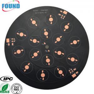
Aluminium PCB Board LED PCB Manufactures Design Electrical Circuits Reverse Engineering Services
Why Choose Us
1) We are the manufacturer/ factory;
2) We have good quality control systems, including ISO 9001, ISO 13485;
3) All the material we use have the UL & RoHS identify;
4) All the components we use are the New & Original;
5) One-stop service can be provided from PCB design, 1-32 layers PCB manufacturing, components sourcing, PCB Assembly, to Fully Product Assembly.
Our Services
1). PCB development and design;
2). PCB manufacturing from 1 to 32 layers(Rigid PCB,Flexible
PCB,Ceramic PCB,Aluminum PCB);
3). PCB Clone;
4). Component sourcing;
5). PCB Assembly;
6). Write program for customers;
7). PCB/ PCBA Test.
| Capability | Standard | Advanced |
| Laminate materials | FR4 / FR1 / CEM-3 / CEM-1 / Aluminum / Flex-rigid /Teflon / High-TG / Rogers / Taconic | |
| Surface Finish | HASL (vertical & Horizontal), Lead Free HASL, HASL+Gold Finger, OSP/Entek, ENIG, ENEPIG, Immersion Tin(ISn) ,Immersion Silver(IAg), Carbon Ink, Hard Gold(Flash Gold), Soft Gold | |
| Min. Thickness for inner layers | 0.020"-0.125" | 0.003”(0.07mm) |
| Board layers | 1-12 Layers | 1-24 Layers |
| Board Thickness | 0.5mm-3mm | 0.2mm-7mm |
| Copper weight | 0.5 oz – 3 oz | 0.5 oz – 8 oz |
| Minimum Trace Width / Spacing | 0.004"/0.004" | 0.003"/0.003" |
| Solder Mask Color | Green,Blue,Black,Red,Yellow,White, and customized | |
| Drill deviation | 0.008" | ±0.002” (0.05mm) |
| PTH hole tolerance | 0.008" | ±0.002” (0.005mm) |
| PTH hole tolerance | 0.008" | ±0.002” (0.005mm) |
| Min hole size | 0.010" | 0.008” (0.02mm) |
| E-test | Flying Probe Tester/Test-Jig/X-ray/ICT/AOI/FCT | |
| Controlled Tolerance | ± 5% | ± 3% |
| Silkscreen Color | White, Black, Yellow, Green, Red, Blue and customized | |
| Min solder mask clearance size | 0.008 | 0.003” (0.07mm) |
| Min silkscreen clearance size | 0.010" | 0.006” (0.15mm) |
| IPC Class | Class 2 | Class 3 |
| Blind Vias | YES | YES |
| Buried Vias | YES | YES |
| Aspect Ratio | 8/1 | 15/1 |
| Carbon Ink | YES | YES |
| Peelable Mask | YES | YES |
Q1:What is your testing policy and how you controle the quality?
A1: For sample, usually tested by flying probe; for PCB Volume over 3 square meters, usually tested by fixture, this will be more faster. Due to there’s many steps to PCB production, we usually do inspection after every step.
Q2:What is your certificate?
A2: ISO/TS16949, ISO14001: 2004, UL, SGS, RoHS report. We can provide the report of raw material based on customer’s requirement.
Q3: What is the lead time?
A3: Sample needs 2-4 working days, mass production needs 7-10 working days. It depends on the files and quantity.
Q4: Do you keep our information and files secret?
A4: Keeping secret for customers is the basic principle of our factory. We can sign with the NDA with you.
Q5: What files should we offer?
A5: If only need PCBs, please provide Gerber File and manufacturing specifications; If need PCBA,Please provide Gerber File, Manufacturing specification, BOM list and Pick & Place/XY file.
Q6: Can we visit your company?
A6: No problem. You are welcome to visit us in Shenzhen.
Aluminium PCB Board LED PCB Manufactures Design Electrical Circuits Reverse Engineering Services


LED PCB Design Aluminum Substrate PCB Electrical Circuits Reverse Engineering Services
Inquiry Cart
0