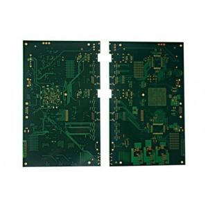
Multilayer Double - Sided HDI PCB OR High Tg PCB OR Heavy Copper PCB Prototyping
Brand Name:Found
Certification:UL E361831
Model Number:FD-100
Minimum Order Quantity:1 pcs
Delivery Time:5-8 work days
Payment Terms:T/T
Contact Now
Add to Cart
Active Member
Location:
Shenzhen Guangdong China
Address:
NO.1 Industry Park, XinSheng Village, Longgang District, ShenZhen
Supplier`s last login times:
within 1 hours
Shipping
lt's easy to get a shipping quote! Just click the button below and complete the short form.
Get Shipping Quote
Product Details
Company Profile
Product Details
Multilayer Double - Sided HDI PCB OR High Tg PCB OR Heavy Copper PCB Prototyping
| Base Materia | FR-4 |
| Board Thickness | 1.2+/-0.12mm |
| size | 190mm*90mm |
| Min. Hole Size | 0.25mm |
| Min. Line Width | 0.12mm |
| Min. Line Spacing | 0.134mm |
| Min. Hole Copper | 22um |
| Copper Thickness | 1OZ |
Product Details
Product Pictures
Product Parameters
| Items | Speci. | |
| Max panel size | 32" x 20.5"(800mm x 520mm) | |
| Min trace width/ space (inner layer) | 4mil/4mil(0.1mm/0.1mm) | |
| Min PAD (inner layer) | 5 mil(0.13mm) | |
| Min thickness(inner layer) | 4 mil(0.1mm) | |
| Inner copper thickness | 1~4 oz | |
| Outer copper thickness | 0.5~6 oz | |
| Finished board thickness | 0.4-3.2 mm | |
Board thickness tolerance control | ±0.10 mm | ±0.10 mm |
| ±10% | ±10% | |
| ±10% | ±10% | |
| Inner layer treatment | brown oxidation | |
| Layer count Capability | 1-30 LAYER | |
| alignment between ML | ±2mil | |
| Min drilling | 0.15 mm | |
| Min finished hole | 0.1 mm | |
| Hole precision | ±2 mil(±50 um) | |
| tolerance for Slot | ±3 mil(±75 um) | |
| tolerance for PTH | ±3 mil(±75um) | |
| tolerance for NPTH | ±2mil(±50um) | |
| Max Aspect Ratio for PTH | 8:1 | |
| Hole wall copper thickness | 15-50um | |
| Alignment of outer layers | 4mil/4mil | |
| Min trace width/space for outer layer | 4mil/4mil | |
| Tolerance of Etching | +/-10% | |
| Thickness of solder mask | on trace | 0.4-1.2mil(10-30um) |
| at trace corner | ≥0.2mil(5um) | |
| On base material | ≤+1.2mil Finished thickness | |
| Hardness of solder mask | 6H | |
| Alignment of solder mask film | ±2mil(+/-50um) | |
| Min width of solder mask bridge | 4mil(100um) | |
| Max hole with solder plug | 0.5mm | |
| Surface finish | HAL (Lead or Lead free), immersion Gold, Immersion Nickel, Electric Gold finger, Electric Gold, OSP, Immersion Silver. | |
| Max Nickel thickness for Gold finger | 280u"(7um) | |
| Max gold thickness for Gold finger | 30u"(0.75um) | |
| Nickel thickness in Immersion Gold | 120u"/240u"(3um/6um) | |
| Gold thickness in Immersion Gold | 2u"/6u"(0.05um/0.15um) | |
| Impedance control and its tolerance | 50±10%,75±10%,100±10% 110±10% | |
| Trace Anti-stripped strength | ≥61B/in(≥107g/mm) | |
| bow and twist | 0.75% | |
advantage:
Over 10 years' manufacturing experience
Assembly provided
100% quality tested before shipment
Certificate of UL, ISO9001, ISO14001 and ISO/TS16949.
Our Products meet the RoHS & WEEE lead-free requirement.
Small Order accepted
3 weeks for massive production; 10 days for sample since material
prepared
Urgent case or spread delivery schedule will be updated per
negociation then
1500mm Long Aluminium PCB Board or Counter Sink Hole...
3D Printers Larid Tpreg 1KA04 Aluminum Clad Hybrid M...
2 Layer Aluminum Heat Emitter Communication PCB OR S...
2 Layers High thermal conductivity aluminum Bergquis...
Advanced Double Sided Flex Lighting Lamp PCB Printed...
High Power LED Driver Rogers Printed Circuit Board P...
- Feedback
Your Name: | |
*E-mail: | |
Phone: | |
Company: | |
Title: | |
*Content: | |
Send |


Multilayer Double - Sided HDI PCB OR High Tg PCB OR Heavy Copper PCB Prototyping
Inquiry Cart
0