Metal Core Aluminium PCB For Led / Led Light Main Printed Circuit Board
Brand Name:Found
Certification:UL E361831 ISO9001 TS16949
Model Number:fd36
Minimum Order Quantity:1PC
Delivery Time:2-8 days
Payment Terms:T/T
Contact Now
Add to Cart
Active Member
Location:
Shenzhen Guangdong China
Address:
NO.1 Industry Park, XinSheng Village, Longgang District, ShenZhen
Supplier`s last login times:
within 1 hours
Shipping
lt's easy to get a shipping quote! Just click the button below and complete the short form.
Get Shipping Quote
Product Details
Company Profile
Product Details
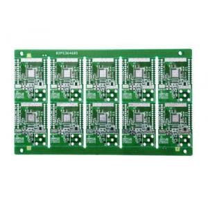
Aluminium PCB Board for Main Printed Circuit Board with LED PCB Board
Pls see our pcb catalog below:
1. single side pcb 2. double side pcb
3. Multilayer pcb(3-26+ layers) 4. Flexible PCB(FPC)
5. Rigid-flex PCB board 6. Aluminum PCB board for LED(1-4 layers)
7. MCPCB board (1-4 layers) 8.Ceramic PCB(1-4 layers)
9. HDI pcb board 10. High frequency PCB
11. PCB assembly
| PCB Description | Our PCB Board Capability | ||
| PCB Surface Finishes | electrolytic nickel-gold, HASL(Lead Free, ENIG (Electroless Nickel/Immersion Gold, Carbon Ink, Golden Fingers, OSP (Entek, Immersion Tin, Immersion Silver | ||
| PCB Max. Size | 1200mm×600mm | ||
| PCB Min. Size | 5mm×5 mm | ||
| Bow & Twist Tolerance | Single Side≤1.0%,Double Side≤0.7%, Muti-Layer≤0.5% | ||
| Min. Board Thickness & Tolerance | 0.2mm±0.08mm | ||
| PCB Min. trace/spacing | Tin board:0.2mm±20%(8mil±0%) | ||
| gold board:0.075mm±20%(3mil±0%) | |||
| Copper to Board Edge Spacing | 0.5mm(20mil) | ||
| Hole to Trace Spacing | 0.3mm(12mil) | ||
| Min. Hole Diameter | 0.2mm±.076mm(8mil±3mil) | ||
| Min. Hole Clearance | 0.4mm±.076mm(16mil±3mil) | ||
| Copper Thickness on Hole Wall | 20-25um(0.79mil-1.0mil) | ||
| Hole Location Tolerance | ±0.076mm(l±3mil) | ||
| Min Diameter of Punching Hole | FR-4 board thickness≤1.0mm(40mil):1.0mm(40mil) | ||
| FR-4 board thickness 1.2-3.0mm(48-120mil):1.5mm(60mil) | |||
| PCB Min. Punching Slot | FR-4 CEM-3 board thickness≤1. 0mm(40mil):0.8 mm×0.8 mm(32mil×32mil) | ||
| FR-4 board thickness1.2-3.0mm(48-120mil): 1.0 mm×1.0 mm(40mil×40mil) | |||
| Trace width variation | ±0.076mm(±3mil) | ||
| Outline Tolerance | Routing:±0.1mm (±4mil) ,Punching:±0.05mm (±2mil) | ||
| V-CUT Registration Tolerance±0.2mm (±8mil) | |||
| PCB BOARD Type | Single-sided, double-sided, multi-layer | ||
| Major Material | FR-4, CEM-1,CEM-3, high frequency laminates, Aluminum, NiFe-based, copper base | ||
| PCB BOARD Thickness | 0.2-3.5mm | ||
| Base Copper Thickness | 11um 35um 70um 105um | ||
| Max. aspect ratio(board thickness: hole size) | 8:1 | ||
| V-Cut Angle Tolerance | ±5° | ||
| V-Cut Board Thickness | 0.4mm -3.2mm(16mil -128mil) | ||
| Min SMT Pitch | 0.3mm(12mil) | ||
| Min. Component mark | 0.15mm(6mil) | ||
| Min. width of annular ring(finished) | 0.15mm(6mil)/side | ||
| Min pad opening | 0.076mm(3mil) | ||
| Min S/M Bridge | ±0.076mm(±3mil) | ||
| carbon ink board manufacturing capability:1.Impedance Control:20K±10% 2.Hardness:6H 3.bearable friction times :above 200000 times | |||
| Technology | |||
| Min trace/space(inner/external) | 3/3 mil0.075/0.075mm | ||
| Min drill size for through hole | drill 8.0 mil0.20mm | ||
| Laser dill | 4 mil0.1mm | ||
| Copper Foil Thickness | 17-210um | ||
| Inner Core Thickness | ±0.08mm | ||
| Tolerance of total board thickness | ±0.015mm | ||
| Max .Unit Area | 700-800 | ||
| Min. Unit Area | 2-5mm | ||
| Max Layer | 1-18 Layers | ||
| Surface Treatment | |||
| Solder Coating Thickness Sn | 4-20um | ||
| Cobalt/ Gold plating, Hard Gold Thickness | Ni:5-10umAu:0.05-0.20um | ||
| Gold/Nickel Plating Thickness | Ni:5-10umAu:0.05-0.15um | ||
| OSP Coating Thickness | 0.2-0.5um | ||
| Electroness Au Thickness | Ni:3-15umAu:0.025-0.10mm | ||
| Chem .Tin Thickness | Sn:0.8-5um | ||
| Producting Capacity | each day :800-100m2 | ||
| Aspect Ratio | 6:01:00 | ||
| Hole Registration | 0.004" (0.1mm) | ||
Trade Terms:
1. Payment: T/T in advance (Western Union , payple is welcomed)
2. Production lead time 100PCS: 5-7days, 500~1000PCS: 7-10days,
above 1000PCS 15-20days.
3. Sample can be delivered in 3days
4. Shipping freight are quoted under your requests
5. Shipping port: Shen zhen,Mainland China
6. Discounts are offered based on order quantities
7. MOQ: 1PCS
Package &Shipping Methods:
1.Vacuum package with silica gel, Carton box with packing belt.
2. By DHL, UPS, FedEx, TNT
3. By EMS (Usually for Russia Clients)
4. By sea for mass quantity according to customer's requirement
| PCB Manufacture Capability | ||
| Item | Manufacture Capability | |
| Layers | 1-26 Layers | |
| HDI | 2+N+2 | |
| Material Types | Fr-4,Fr-5,High-Tg,Aluminum Based , Halogen Free, | |
| Isola,Taconic,Arlon,Teflon,Rogers, | ||
| Max.Panel Dimension | 39000mil * 47000mil (1000mm * 1200mm) | |
| Outline Tolerance | ± 4mil (± 0.10mm) | |
| Board Thickness | 8mil-236mil (0.2 - 6.0mm) | |
| Board Thickness Tolerance | ± 10% | |
| Dielectric Thickness | 3mil-8mil ( 0.075mm-0.20mm) | |
| Min.Track Width | 3mil ( 0.075mm ) | |
| Min.Track Space | 3mil ( 0.075mm ) | |
| External Cu Thickness | 0.5 OZ - 10 OZ ( 17um - 350um) | |
| Internal Cu Thickness | 0.5OZ - 6OZ ( 17um - 210um) | |
| Drilling Bit Size ( CNC ) | 6mil-256mil ( 0.15mm - 6.50mm) | |
| Finished Hole Dimension | 4mil-236mil(0.1mm - 6.0mm) | |
| Hole Tolerance | ± 2mil (± 0.05mm) | |
| Laser Drilling Hole Size | 4mil(0.1mm) | |
| Aspect Ration | 16: 1 | |
| Solder Mask | Green,Blue,White,Black,Red,Yellow,Purple,etc. | |
| Min Solder mask Bridge | 2mil(0.050mm) | |
| Plugged Hole Diameter | 8mil-20mil ( 0.20mm-0.50mm) | |
| Beveling | 30o - 45o | |
| V-scoring | +/-0.1mm,15o30o45o60o | |
| Impedance Control | Min. 5%General10% | |
| Surface Finishing | HASL,HASL(lead Free),Immersion Gold | |
| Immersion Silver,OSP,Hard Gold ( up to 100u" ) | ||
| Certification | UL RoHS ISO9001: 2000 ISO14000: 2004 SGS | |
| Quality Standards | Accept spcifications of customer and IPC(class II or III) | |
Features and benefits
1. The dielectric constant (DK) is low and stable, so the signal
transmission is good without delay.
2. The characteristic of low dielectric loss makes the signal loss
at a lower level, which makes the signal
transmission of the whole equipment excellent.
3. Delamination of copper foil will not be caused by the change of
cold and heat due to the consistency
with the thermal expansion coefficient of copper foil.
4. Immersion gold has excellent surface planarity, particularly
helpful for PCBs with BGA packages or even CSP mounted components
to reduce failure rate during assembly and soldering.
5. UL, ISO certified PCB manufacturing factory.
6. Make delivery on time keeping 98% on-time-delivery rate.
7. Eligible products rate of first production: >95%
8. Experienced sales persons provide skilled customer services.
9. Fast and flexible to save the time of production from prototype
to standard production


Metal Core Aluminium PCB For Led / Led Light Main Printed Circuit Board
Inquiry Cart
0