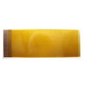
2 Layers FPC 0.15MM Yellow PCB and flexible printed circuit boards
Brand Name:Found
Certification:UL:E361831
Model Number:Found94
Minimum Order Quantity:1PC
Delivery Time:2-8 days
Payment Terms:T/T
Contact Now
Add to Cart
Active Member
Location:
Shenzhen Guangdong China
Address:
NO.1 Industry Park, XinSheng Village, Longgang District, ShenZhen
Supplier`s last login times:
within 1 hours
Shipping
lt's easy to get a shipping quote! Just click the button below and complete the short form.
Get Shipping Quote
Product Details
Company Profile
Product Details
2 Layers FPC 0.15MM Yellow PCB and flexible printed circuit boards
| PCB Description | Our PCB Board Capability | ||
| PCB Surface Finishes | electrolytic nickel-gold, HASL(Lead Free, ENIG (Electroless Nickel/Immersion Gold, Carbon Ink, Golden Fingers, OSP (Entek, Immersion Tin, Immersion Silver | ||
| PCB Max. Size | 1200mm×600mm | ||
| PCB Min. Size | 5mm×5 mm | ||
| Bow & Twist Tolerance | Single Side≤1.0%,Double Side≤0.7%, Muti-Layer≤0.5% | ||
| Min. Board Thickness & Tolerance | 0.2mm±0.08mm | ||
| PCB Min. trace/spacing | Tin board:0.2mm±20%(8mil±0%) | ||
| gold board:0.075mm±20%(3mil±0%) | |||
| Copper to Board Edge Spacing | 0.5mm(20mil) | ||
| Hole to Trace Spacing | 0.3mm(12mil) | ||
| Min. Hole Diameter | 0.2mm±.076mm(8mil±3mil) | ||
| Min. Hole Clearance | 0.4mm±.076mm(16mil±3mil) | ||
| Copper Thickness on Hole Wall | 20-25um(0.79mil-1.0mil) | ||
| Hole Location Tolerance | ±0.076mm(l±3mil) | ||
| Min Diameter of Punching Hole | FR-4 board thickness≤1.0mm(40mil):1.0mm(40mil) | ||
| FR-4 board thickness 1.2-3.0mm(48-120mil):1.5mm(60mil) | |||
| PCB Min. Punching Slot | FR-4 CEM-3 board thickness≤1. 0mm(40mil):0.8 mm×0.8 mm(32mil×32mil) | ||
| FR-4 board thickness1.2-3.0mm(48-120mil): 1.0 mm×1.0 mm(40mil×40mil) | |||
| Trace width variation | ±0.076mm(±3mil) | ||
| Outline Tolerance | Routing:±0.1mm (±4mil) ,Punching:±0.05mm (±2mil) | ||
| V-CUT Registration Tolerance±0.2mm (±8mil) | |||
| PCB BOARD Type | Single-sided, double-sided, multi-layer | ||
| Major Material | FR-4, CEM-1,CEM-3, high frequency laminates, Aluminum, NiFe-based, copper base | ||
| PCB BOARD Thickness | 0.2-3.5mm | ||
| Base Copper Thickness | 11um 35um 70um 105um | ||
| Max. aspect ratio(board thickness: hole size) | 8:1 | ||
| V-Cut Angle Tolerance | ±5° | ||
| V-Cut Board Thickness | 0.4mm -3.2mm(16mil -128mil) | ||
| Min SMT Pitch | 0.3mm(12mil) | ||
| Min. Component mark | 0.15mm(6mil) | ||
| Min. width of annular ring(finished) | 0.15mm(6mil)/side | ||
| Min pad opening | 0.076mm(3mil) | ||
| Min S/M Bridge | ±0.076mm(±3mil) | ||
| carbon ink board manufacturing capability:1.Impedance Control:20K±10% 2.Hardness:6H 3.bearable friction times :above 200000 times | |||
| Technology | |||
| Min trace/space(inner/external) | 3/3 mil0.075/0.075mm | ||
| Min drill size for through hole | drill 8.0 mil0.20mm | ||
| Laser dill | 4 mil0.1mm | ||
| Copper Foil Thickness | 17-210um | ||
| Inner Core Thickness | ±0.08mm | ||
| Tolerance of total board thickness | ±0.015mm | ||
| Max .Unit Area | 700-800 | ||
| Min. Unit Area | 2-5mm | ||
| Max Layer | 1-18 Layers | ||
| Surface Treatment | |||
| Solder Coating Thickness Sn | 4-20um | ||
| Cobalt/ Gold plating, Hard Gold Thickness | Ni:5-10umAu:0.05-0.20um | ||
| Gold/Nickel Plating Thickness | Ni:5-10umAu:0.05-0.15um | ||
| OSP Coating Thickness | 0.2-0.5um | ||
| Electroness Au Thickness | Ni:3-15umAu:0.025-0.10mm | ||
| Chem .Tin Thickness | Sn:0.8-5um | ||
| Producting Capacity | each day :800-100m2 | ||
| Aspect Ratio | 6:01:00 | ||
| Hole Registration | 0.004" (0.1mm) | ||
Features and benefits
1. The dielectric constant (DK) is low and stable, so the signal
transmission is good without delay.
2. The characteristic of low dielectric loss makes the signal loss
at a lower level, which makes the signal
transmission of the whole equipment excellent.
3. Delamination of copper foil will not be caused by the change of
cold and heat due to the consistency
with the thermal expansion coefficient of copper foil.
4. Immersion gold has excellent surface planarity, particularly
helpful for PCBs with BGA packages or even CSP mounted components
to reduce failure rate during assembly and soldering.
5. UL, ISO certified PCB manufacturing factory.
6. Make delivery on time keeping 98% on-time-delivery rate.
7. Eligible products rate of first production: >95%
8. Experienced sales persons provide skilled customer services.
9. Fast and flexible to save the time of production from prototype
to standard production
Product Details
2 layers FPC 0.15MM yellow PCB
Hot Tags: 2 layers fpc 0.15mm yellow pcb, China, factory,
manufacturers, suppliers, quotation, made in China
6 Layers ENIG PCB Heavy Copper PCB
Heavy Copper Fr-4 Multilayer Pcb Board Through Hole ...
Fr4 Electronic Foil Metal Composite Materials Assemb...
Long Led Pcba
3-8 Layer Gold Finger Multi-Layer Flex PCB Design Hi...
MC PCB Aluminum Bergquist T-Clad Ims PCB
- Feedback
Your Name: | |
*E-mail: | |
Phone: | |
Company: | |
Title: | |
*Content: | |
Send |


2 Layers FPC 0.15MM Yellow PCB and flexible printed circuit boards
Inquiry Cart
0