HF Prototype PCB Board High Frequency Prototype Printed Circuit Board
Brand Name:OEM and ODM
Certification:UL,RoHS, CE
Model Number:SL80813S001
Minimum Order Quantity:1pc
Delivery Time:5-7 days
Payment Terms:T/T, Western Union, MoneyGram,Paypal
Contact Now
Add to Cart
Verified Supplier
Location:
Shenzhen Guangdong China
Address:
Room 201 Building A2 Industrial Park No. 6 Yuanchuang Park Rongfu road, Fucheng Street Longhua District Shenzhen City 518131
Supplier`s last login times:
within 25 hours
Shipping
lt's easy to get a shipping quote! Just click the button below and complete the short form.
Get Shipping Quote
Product Details
Company Profile
Product Details
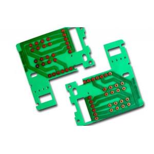
HF PCB, High frequency printed circuit board for RF antenna Taconic
RF Antenna PCB information:
PCB Specification:
Layer of number | 4 | Surface finish | ENIG |
Base material | Taconic | Cu THK | 1OZ |
Board THK | 0.8mm | Origin | Shenzhen |
Board size | 12*6cm | Solder mask | Green |
Antenna pcb including:
GSM 3G antenna PCB, quad band antenna PCB, multil band antenna PCB,WIFI antenna pcb
Satellite antenna pcb, Car antenna pcb, GPS antenna pcb, GSM antenna pcb, Radar antenna pcb, FM/AM antenna pcb,2.4GHZ antenna pcb
We can offer production with high quality and competitive
Item | Mass Production | Pilot Run Production |
Capacity | Capacity | |
Layer Counts | 1L_18L, HDI | 20-28 , HDI |
Material | FR4 | |
Teflon,PTFE(F4B,F4BK), Rogers(4003,4350,5880) Taconic(TLX-8,TLX-9), Arlon(35N,85N)etc. | ||
Material Mixed Laminate | 4 layers -- 10 layers | 12 layers |
FR4+Ro4350 , Rogers3003+FR4 | ||
Maximum Size | 610mm X 1200mm | 1200 - 2000MM |
Board Outline Tolerance | ±0.15mm | ±0.10mm |
Board Thickness | 0.125mm--6.00mm | 0.1mm--8.00mm |
Thickness Tolerance ( t≥0.8mm) | ± 8% | ±5% |
Thickness Tolerance( t<0.8mm) | ±10% | ±8% |
Minimum Line / Space | 0.10mm | 0.075mm |
Trace width Tolerance | 15%-20% | 10% |
Minimum Drilling Hole (Mechanical) | 0.2mm | 0.15mm |
Minimum laser hole | 0.1mm | 0.075mm |
Hole Position/hole Tolerance | ±0.05mm PTH:±0.076MM NPTH:±0.05mm | |
Mini hole ring (single | 0.075MM | 0.05MM |
OutLayer Copper Thickness | 17um--175um | 175um--210um |
InnerLayer Copper Thickness | 17um--175um | 175um--210um |
Mini Solder Mask Bridge | 0.05mm | 0.025mm |
Impedance Control Tolerance | ±10% | ±5% |
Surface Finishing | HASL, Lead free HASL, Immersion gold, Immersion tin, Immersion Silver. | |
Plated gold , OSP, Carbon ink, | ||
1-2L Lead-time | 3-7 days | 1-2 days |
4- 8L Lead-time | 7-10 days | 2-7 days |
10-18L Lead-time | 10-15 days | 4-9 days |
20-28L Lead-time | 15-20 days | |
Acceptable File Format | ALL Gerber Files,POWERPCB,PROTEL,PADS2000,CAD,AUTOCAD,ORCAD,P-CAD,CAM-350,CAM2000 etc. | |
Quality Standards | IPC-A-600F and MIL-STD-105D CHINA GB<4588> | |
PCB Picture

HF Prototype PCB Board High Frequency Prototype Printed Circuit Board
Inquiry Cart
0