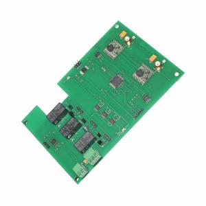
100% E-Test ISO Qualified Pcba Pcb Circuit Board Multilayer Printed Circuit Board
Brand Name:OEM/ODM
Certification:UL,RoHS, CE
Model Number:SL80224S010
Minimum Order Quantity:1pc
Delivery Time:5-7 days
Payment Terms:T/T, Western Union, MoneyGram,Paypal
Contact Now
Add to Cart
Verified Supplier
Location:
Shenzhen Guangdong China
Address:
Room 201 Building A2 Industrial Park No. 6 Yuanchuang Park Rongfu road, Fucheng Street Longhua District Shenzhen City 518131
Supplier`s last login times:
within 25 hours
Shipping
lt's easy to get a shipping quote! Just click the button below and complete the short form.
Get Shipping Quote
Product Details
Company Profile
Product Details
100% E-Test ISO Qualified Pcba Pcb Circuit Board Multilayer Printed
Circuit Board
1. PCB fabrication.
2. One-stop PCBA: PCB+components sourcing+SMD and through-hole assembly
3. PCB clone, PCB reverse engineering.
Files Requested For PCB Assembly Quotation
---In order to provide you with the most efficient and accurate
quote on manufacturing the requested unit, we ask that you provide
us with the following information.
1. Gerber file,PCB file,Eagle file or CAD file are all acceptable
2. A detailed bill of materials (BOM)
3. Clear pictures of PCB or PCBA sample for us
4. Quantity and delivery required
5. Test method for PCBA to guarantee 100% good quality products.
6. Schematics file for PCB design if need to do function test.
7. A sample if available for better sourcing
8. CAD files for enclosure manufacturing if required
9. A complete wiring and assembly drawing showing any special
assembly instructions if required
Shinelink kinds PCBA Products
Feature
| Number of Layer | 1 - 20 Layer |
| Maximum Processing Area | 680 × 1000MM |
| Min Board Thickness | 2 Layer - 0.3MM ( 12 mil ) |
| 4 Layer - 0.4MM ( 16 mil ) | |
| 6 Layer - 0.8MM ( 32 mil ) | |
| 8 Layer - 1.0MM ( 40 mil) | |
| 10 Layer - 1.1MM ( 44 mil ) | |
| 12 Layer - 1.3MM ( 52 mil ) | |
| 14 Layer - 1.5MM ( 59 mil ) | |
| 16 Layer - 1.6MM ( 63 mil ) | |
| 18 Layer - 1.8MM ( 71 mil ) | |
| Finished Board Thickness Tolerance | Thickness ≤ 1.0MM, Tolerance: ± 0.1MM |
| 1.0MM ≤ Thickness ≤ 6.5MM, Tolerance ± 10% | |
| Twisting and Bending | ≤ 0.75%, Min: 0.5% |
| Range of TG | 130 - 215 ℃ |
| Impedance Tolerance | ± 10%, Min: ± 5% |
| Hi-Pot Test | Max: 4000V/10MA/60S |
| Surface Treatment | HASL, With Lead, HASL Free Lead |
| Flash Gold, Immersion Gold | |
| Immersion Silver, Immersion Tin | |
| Gold Finger, OSP |
PCB Assembly Capabilities
| Turnkey PCBA | PCB+components sourcing+assembly+package |
| Assembly details | SMT and Thru-hole, ISO lines |
| Lead Time | Prototype: 15 work days. Mass order: 20~25 work days |
| Testing on products | Flying Probe Test, X-ray Inspection, AOI Test, functional test |
| Quantity | Min quantity: 1pcs. Prototype, small order, mass order, all OK |
| Files we need | PCB: Gerber files(CAM, PCB, PCBDOC) |
| Components: Bill of Materials(BOM list) | |
| Assembly: Pick-N-Place file | |
| PCB panel Size | Min size: 0.25*0.25 inches(6*6mm) |
| Max size: 20*20 inches(500*500mm) | |
| PCB Solder Type | Water Soluble Solder Paste, RoHS lead free |
| Components details | Passive Down to 0201 size |
| BGA and VFBGA | |
| Leadless Chip Carriers/CSP | |
| Double-sided SMT Assembly | |
| Fine Pitch to 0.8mils | |
| BGA Repair and Reball | |
| Part Removal and Replacement | |
| Component package | Cut Tape,Tube,Reels,Loose Parts |
| PCB assembly process | Drilling-----Exposure-----Plating-----Etaching & Stripping-----Punching-----Electrical Testing-----SMT-----Wave Soldering-----Assembling-----ICT-----Function Testing-----Temperature & Humidity Testing |
FAQ
1. What service can you provide?
We can provide PCB circuit board gerber file design,Copy and
Clone,OEM and ODM service.Not only produce PCB,PCB Assembly,but
also Mold making ,Plastic Injection,and Complete products
2. Are my design files secure when I send them to you?
Your files are held in complete safety and security while Shinelink
Technology Ltd is in possession of them. Your files are never
shared nor will any third parties have access to your design files.
Since they are your property, we respect the copyright of your
files. The customer controls the disposition of these files per
your requirements and written approval.
3. For small quantity orders, can you produce prototype PCBs?
Yes. Shinelink Technology Ltd has the capability to produce circuit
boards in any amount. But,the greater the quantity, the greater the
cost savings.
4. What’s the typical process flow for multi-layer PCB?
Material cutting → Inner dry film → inner etching → Inner AOI → Multi-bond→ Layer stack up Pressing → Drilling → PTH → Panel Plating → Outer Dry Film → Pattern Plating → Outer etching → Outer AOI → Solder Mask → Component Mark → Surface finish → Routing → E/T → Visual Inspection.
5. What’s the key equipments for HDI manufacturing?
Key equipment list is as following: Laser drilling machine, Pressing machine, VCP line, Automatic Exposing machine, LDI and etc.
The equipments we have are the best in the industry, laser drilling machines are from Mitsubishi and Hitachi, LDI machines are from Screen(Japan), Automatic Exposing machines are also from Hitachi, all of them make we can meet customer’s technical requirements.

100% E-Test ISO Qualified Pcba Pcb Circuit Board Multilayer Printed Circuit Board
Inquiry Cart
0