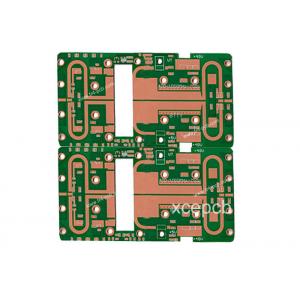
Impedance Control Prototype PCB Boards Green 1.0MM Blink / Buried
Brand Name:XCE
Certification:CE,ROHS, FCC,ISO9008,SGS,UL
Model Number:XCEP
Minimum Order Quantity:1pcs
Delivery Time:5-10 days
Payment Terms:T/T,Western union
Contact Now
Add to Cart
Site Member
Location:
Shenzhen Guangdong China
Address:
Room 403 Block A,Huafeng SOHO Creative World Hangcheng Industrial Zone Qianjin 2nd Road,Xixiang Baoan Shenzhen,China
Supplier`s last login times:
within 27 hours
Shipping
lt's easy to get a shipping quote! Just click the button below and complete the short form.
Get Shipping Quote
Product Details
Company Profile
Product Details
Impedance Control Prototype PCB Boards Green 1.0MM Blink / Buried
Application:
Automobile
Backplanes
Servers and Networking
Telecommunications
Data Storage
Heavy Copper Application
Specification:
| Base Material: fr4 |
| Layer:2 |
| Thickness: 1.0MM |
| Copper weight:2OZ |
| Surface finish: ENIG |
High frequency:
| Model | Parameter | thickness(mm) | Permittivity(ER) |
| F4B | F4B | 0.38 | 2.2 |
| F4B | 0.55 | 2.23 | |
| F4B | 0.225,0.3,0.5,08,1,1.2,1.5,2,2.5,3.0 | 2.65 | |
| F4Bk | 0.8,1.5 | 2.65 | |
| F4B | 0.8 | 3.5 | |
| FE=F4BM | 1 | 2.2 | |
| Rogers | RO5880 | 0.254 0.508 0.762 | 2.20 ± 0.02 |
| RO4350 | 0.254 0.508,0.8,1.524 | 3.5 | |
| RO4003 | 0.508 | 3.38 | |
| TACONIC | TLF-35 | 0.8 | 3.5 |
| TLA-6 | 0.254,0.8,1,1.5, | 2.65 | |
| TLX-8 | 0.254,0.8,1,1.6 | 2.55 | |
| RF-60A | 0.64 | 6.15 | |
| TLY-5 | 0.254,0.508,0.8 | 2.2 | |
| TLC-32 | 0.8,1.5,3 | 3.2 | |
| TLA-35 | 0.8 | 3.2 | |
| ARLON | AD255C06099C | 1.5 | 2.55 |
| MCG0300CG | 0.8 | 3.7 | |
| AD0300C | 0.8 | 3 | |
| AD255C03099C | 0.8 | 2.55 | |
| AD255C04099C | 1 | 2.55 | |
| DLC220 | 1 | 2.2 |
Specification:
Technology | Materials |
|
|
PCB thickness | Final copper |
|
|
Conductor track widths | Minimum drilling diameter |
|
|
Contour production | Solder masks |
|
|
Surfaces | Additional printing |
|
|
Layer | 12-26 |
Material type | FR-4, CEM-1, CEM-3, High TG, FR4 Halogen Free, Rogers |
Board thickness | 0.21mm to 7.0mm |
Copper thickness | 0.5 OZ to 6 oz |
Size | Max. Board Size: 580mm×1100mm |
Min. Drilled Hole Size: 0.2 mm (8 mil) | |
Min. Line Width: 4mil (0.1mm) | |
Min. Line Spacing: 4mil (0.1mm) | |
Surface finishing | HASL / HASL lead free, HAL, Chemical tin, |
Solder Mask Color | Green/Yellow/Black/White/Red/Blue |
Tolerance | Shape tolerance: ±0.13 |
Hole tolerance: PTH: ±0.076 NPTH: ±0.05 | |
Certificate | UL, ISO 9001, ISO 14001 |
Special requirements | Buried and blind vias+controlled impedance +BGA |
Profiling | Punching, Routing, V-CUT, Beveling |
Why us ?
1)Professional engineer team --help you to check design and do engineering before production |
2)Rich expierences in pcb production industry--provide high quality and competitive price pcb. |
3) After-sales service--every problem you have will get our professional advice and solution. |
4) Constant follow up-- make us have the fast reaction of your requirement. |
5) Inspected by the Inspection Institution--ISO,UL,ROHS cerfiticated |
Our PCB - Printed Circuit Board capabilities include:
- One to Thirty Layers
- Rigid Flex Circuit Board
- One to Eight layer flexible PCB
- Hybrid constructions PCB
- Metal core (Aluminum)
- PCB up to 6 oz inner layer
- Finishes: HASL, HASL (Pb-free), Soft Bondable Gold, Electrolytic Gold, Immersion Gold, Immersion Silver, Immersion Tin, OSP.
- Materials: Polyimide, Arlon, Nelco, Rogers, Getek, Polyclad
- Impedance Control and Blink/Buried Vias, HDI, Microvias
- RoHS Compliant (RoHS – Restrictions on the use Of Hazardous Substances)

Impedance Control Prototype PCB Boards Green 1.0MM Blink / Buried
Inquiry Cart
0