0.79MM Thickness Rogers 4350B PCB Board Without Soldermask For Microwave / RF
Brand Name:XCE
Certification:CE,ROHS, FCC,ISO9008,SGS,UL
Model Number:XCEM
Minimum Order Quantity:1pcs
Delivery Time:5-10 days
Payment Terms:T/T,Western union
Contact Now
Add to Cart
Site Member
Location:
Shenzhen Guangdong China
Address:
Room 403 Block A,Huafeng SOHO Creative World Hangcheng Industrial Zone Qianjin 2nd Road,Xixiang Baoan Shenzhen,China
Supplier`s last login times:
within 27 hours
Shipping
lt's easy to get a shipping quote! Just click the button below and complete the short form.
Get Shipping Quote
Product Details
Company Profile
Product Details
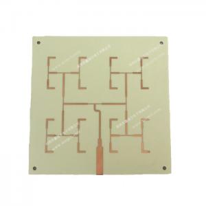
Rogers4350B Board Without Soldermask For Microwave/RF Applications
0.79MM Thickness
Specifiction:
layer:6
board thickness:0.79mm
Copper thickness:1oz
min Hole size:0.2mm
min line width and distance:5/5mil
Surface treatment: imersion Tin
Application: Microwave/RF
Product Description
L1-L2 Blind holes;
L2-L3 Bury holes;
L1-L4 Through holes;
Copper based with Rogers 4350 T1.3mm.
Copper thickness 0.70mm;
Milling thickness 1.2mm.
Description :
RO4350B materials are proprietary woven glass reinforced
hydrocarbon/ceramics with electrical performance close to
PTFE/woven glass and the manufacturability of epoxy/ glass.
Providing tight control on dielectric constant and low loss while
utilizing the same processing method as standard epoxy/glass,
RO4350B is available at a fraction of the cost of conventional
microwave laminates. No special through-hole treatments or handling
procedures are required as with PTFE based microwave materials.
RO4350B materials are UL 94V-0 rated for active devices and high
power RF designs.
Specification
| PCB Type: | Rogers PCB |
| Layer : | 6 layer |
| Min .Line Width/Space: | 5mil/5mil |
| Min. Via Diameter: | 0.3mm |
| Finish Thickness: | 0.2mm |
| Surface Finish: | Immersion Tin |
| Size: | 101*150MM |
| Material: | Rogers |
| Color: | / |
| Application | Microwave/RF |
Rogers material in stock:
| Brand | Model | Thickness(mm) | DK(ER) |
| F4B | F4B | 0.38 | 2.2 |
| F4B | 0.55 | 2.23 | |
| F4B | 0.225,0.3,0.5,08,1,1.2,1.5,2,2.5,3.0 | 2.65 | |
| F4Bk | 0.8,1.5 | 2.65 | |
| F4B | 0.8 | 3.5 | |
| FE=F4BM | 1 | 2.2 | |
| Rogers | RO4003 | 0.254 0.508,0.813,1.524 | 3.38 |
| RO4350 | 0.254 0.508,0.762,1.524 | 3.5 | |
| RO5880 | 0.254.0.508.0.762 | 2.2 | |
| RO3003 | 0.127,0.508,0.762,1.524 | 3 | |
| RO3010 | 0.635 | 10.2 | |
| RO3206 | 0.635MM | 10.2 | |
| R03035 | 0.508MM | 3.5 | |
| RO6010 | 0.635MM, 1,27MM | 10.2 |
Our PCB board manufacture
* PCB board file with parts list provided by customers
* PCB board made, circuit board parts purchased by us
* Electronic testing circuit board
* Fast delivery, anti-static package
* RoHS Directive-compliant, lead-free
Testing Procedures For PCB Board
---We perform multiple quality assuring procedures before shipping
out any PCB board. These include:
* Visual Inspection
* Flying probe
* Bed of nails
· * Impedance control
· * Solder-ability detection
* Digital metallograghic microscope
· *AOI (Automated Optical Inspection)
Available substrates:
RO4350B RO4003C TLX-8 (TACONIC) F4B Woven Glass-Reinforced PTFE
4mil(0.1mm) 8mil (0.203mm) 20mil(0.5mm)
10mil(0.254mm) 12mil(0.3mm) 30mil(0.762mm)
13.3mil(0.338mm) 20mil(0.508mm) 40mil(1.0mm)
20mil (0.508mm) 32mil(0.813mm)
30mil(0.762mm) 60mil(1.524mm)
60mil(1.524mm)
Applications:
Amplifier Combiner Coupler Mixer Multiplexer Power divider WiFi
WiMAX, LTE bands 3G and 4G antenna
Competitive Advantage:
1) With UL,ROHS,ISO,IPC
2).Lead time:3-10 working days
3)Competitive price best quality
4).Rich 20 years experience in High Tg Multilayer PCB .
What Information customer need to provide for quotation ?
1. PCB Gerber files ,protel,powerpcb,Autocad,etc.
2. BOM list for PCB assembly.
3. Send us your sample PCB or PCBA.
4. OEM is acceptable.

0.79MM Thickness Rogers 4350B PCB Board Without Soldermask For Microwave / RF
Inquiry Cart
0