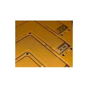
Polyimide Material Flexible Circuit Board PCB Model.No HSFPC10012 With 2 layers
Brand Name:HUASWIN
Certification:ISO/UL/RoHS
Model Number:HSFPC10012
Minimum Order Quantity:1 sets
Delivery Time:7-12 working days
Payment Terms:T/T, Western Union, L/C
Contact Now
Add to Cart
Active Member
Supplier`s last login times:
within 1 hours
Shipping
lt's easy to get a shipping quote! Just click the button below and complete the short form.
Get Shipping Quote
Product Details
Company Profile
Product Details
Polyimide Material Flexible Circuit Board PCB Model.No HSFPC10012 With 2 layers Finished Copper 1OZ Thickness 0.25mm
FAQ
Q: What files do you use in PCB fabrication?
A: Gerber or Eagle, BOM listing, PNP and Components Position
Q:Is it possible you could offer sample?
A: Yes, we can custom you sample to test before mass production
Q: When will I get the quotation after sent Gerber, BOM and test
procedure?
A: Within 6 hours for PCB quotation and around 24-48 hours for PCBA
quotation.
Q: How can I know the process of my PCB production?
A: 5-7days for PCB production and components purchasing, and 14
days for PCB assembly and Testing
Q: How can I make sure the quality of my PCB?
A: We ensure that each piece of PCB products work well before
shipping. We'll test all of them according to your test procedure.
Detailed Specification of Flexible PCB Manufacturing
Technical Specification | ||
Layers: | 1~10 (flex Pcb) and 2~8 (rigid flex) |
|
Min Panel Size: | 5mm x 8mm |
|
Max Panel Size: | 250 x 520mm |
|
Min Finished board thickness: | 0.05mm (1 sided inclusive copper) |
|
Max Finished board thickness: | 0.3mm (2 sided inclusive copper) |
|
Finished board thickness tolerance: | ±0.02~0.03mm |
|
Material: | Kapton, Polyimide, PET |
|
Base copper thickness (RA or ED): | 1/3 oz, 1/2 oz, 1oz, 2oz |
|
Base PI thickness: | 0.5mil, 0.7mil, 0.8mil, 1mil, 2mil |
|
Stiffner: | Polyimide, PET, FR4, SUS |
|
Min Finished hole diameter: | Φ 0.15mm |
|
Max Finished hole diameter: | Φ 6.30mm |
|
Finished hole diameter tolerance (PTH): | ±2 mil ( ±0.050mm) |
|
Finished hole diameter tolerance (NPTH): | ±1 mil ( ±0.025mm) |
|
Min width/spacing (1/3oz): | 0.05mm/0.06mm |
|
Min width/spacing (1/2oz): | 0.06mm/0.07mm |
|
Min width/spacing (1oz): | Single layer: 0.07mm/0.08mm |
|
Double layer: 0.08mm/0.09mm |
| |
Aspect Ratio | 6:01 | 8:01 |
Base Copper | 1/3Oz--2Oz | 3 Oz for Prototype |
Size Tolerance | Conductor Width:±10% | W ≤0.5mm |
Hole Size: ±0.05mm | H ≤1.5mm | |
Hole Registration: ±0.050mm |
| |
Outline Tolerance:±0.075mm | L ≤50mm | |
Surface Treatment | ENIG: 0.025um - 3um |
|
OSP: |
| |
Immersion Tin: 0.04-1.5um |
| |
Dielectric Strength | AC500V |
|
Solder Float | 288℃/10s | IPC Standard |
Peeling Strength | 1.0kgf/cm | IPC-TM-650 |
Flammability | 94V-O | UL |
PCB Assembly services:
SMT Assembly
Automatic Pick & Place
Component Placement as Small as 0201
Fine Pitch QEP - BGA
Automatic Optical Inspection
Through-hole Assembly
Wave Soldering
Hand Assembly and Soldering
Material Sourcing
IC pre-programming / Burning on-line
Function testing as requested
Aging test for LED and Power boards
Complete unit assembly (which including plastics, metal box, Coil,
cable assembly etc)
Packing design
Conformal coating
Both dip-coating and vertical spray coating is available.
Protecting non-conductive dielectric layer that is
applied onto the printed circuit board assembly to protect the
electronic assembly from damage due to
contamination, salt spray, moisture, fungus, dust and corrosion
caused by harsh or extreme environments.
When coated, it is clearly visible as a clear and shiny material.
Complete box build
Complete 'Box Build' solutions including materials management of
all components, electromechanical parts,
plastics, casings and print & packaging material
Testing Methods
AOI Testing
· Checks for solder paste
· Checks for components down to 0201"
· Checks for missing components, offset, incorrect parts, polarity
X-Ray Inspection
X-Ray provides high-resolution inspection of:
· BGAs
· Bare boards
In-Circuit Testing
In-Circuit Testing is commonly used in conjunction with AOI
minimizing functional defects caused by
component problems.
· Power-up Test
· Advanced Function Test
· Flash Device Programming
· Functional testing
Description
Your Best Choice for Flex PCB and Rigid-flex PCB Manufacturing
& Assembly
ADVANTAGES:
We product all kinds of Flex pcb and Rigid flex pcb which are
widely used in modern portable electronics and devices. Such as
Cell pone, key board, LCD module, Disk cable and etc.
1. With 15 years experience in circuit board, Printed Circuit Board
field to serve your needs
2. Competitive circuit board, Printed Circuit Board price with high
quality
3. Excellent service and prompt delivery
4. Our circuit board, Printed Circuit Board get ISO and UL
Certificates and meet ROHS REACH standard
1. Professional & experienced engineers
2. Competitive price
3. In time service
4. Product warranty
Detailed Specification of Pcb Assembly
1 | Type of Assembly | SMT and Thru-hole |
2 | Solder Type | Water Soluble Solder Paste,Leaded and Lead-Free |
3 | Components | Passives Down to 0201 Size |
BGA and VFBGA | ||
Leadless Chip Carries/CSP | ||
Double-Sided SMT Assembly | ||
Fine Pitch to 08 Mils | ||
BGA Repair and Reball | ||
Part Removal and Replacement-Same Day Service | ||
3 | Bare Board Size | Smallest:0.25x0.25 Inches |
Largest:20x20 Inches | ||
4 | File Formats | Bill of Materials |
Gerber Files | ||
Pick-N-Place File(XYRS) | ||
5 | Type of Service | Turn-Key,Partial Turn-Key or Consignment |
6 | Component Packaging | Cut Tape |
Tube | ||
Reels | ||
Loose Parts | ||
7 | Turn Time | 15 to 20 days |
8 | Testing | AOI inspection |
X-Ray inspection | ||
In-Circuit testing | ||
Functional test |


Polyimide Material Flexible Circuit Board PCB Model.No HSFPC10012 With 2 layers
Inquiry Cart
0