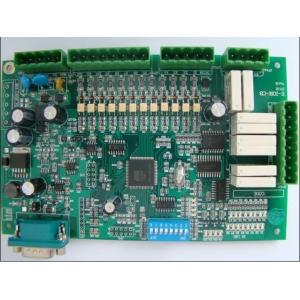
Multi Layer Turnkey PCB Assembly / Prototype Printed Circuit Boards Assembly
Brand Name:HUASWIN
Certification:ISO/UL/RoHS
Model Number:HSPCBA1001
Minimum Order Quantity:1 sets
Delivery Time:15-20 working days
Payment Terms:T/T, Western Union, L/C
Contact Now
Add to Cart
Active Member
Supplier`s last login times:
within 1 hours
Shipping
lt's easy to get a shipping quote! Just click the button below and complete the short form.
Get Shipping Quote
Product Details
Company Profile
Product Details
Multi Layer Turnkey PCB Assembly / Prototype Printed Circuit Boards Assembly
Specifications
1. Electronics PCB and PCB assembly manufacturer
2. UL,RoHS,SGS, ISO Approved
3. Reliable OEM / ODM PCB assembly
4. High Quality, fast delivery
Huaswin Electronics offers customer two options when it comes to PCB Assembly Services, Full or Partial
Turn-Key PCB Assembly service.
Full Turn-Key service takes care of the entire process including PCB Fabrication, Component Procurement,
PCB Assembly and testing. For customers who do not require the full Turn-Key solution then Partial Turn-Key
will fit the bill.
With Partial Turn-Key, you provide the blank PCBs and we assemble according to your requirements. You have
the option of providing some or all of the components, and Huaswin’s dedicated Procurement team will assist
with any remaining parts.
Welcome to Huaswin!
Huaswin Electronics is a professional PCB & PCB Assembly manufacturer, located in Shenzhen, China.
We supply one-stop facility services: PCB design, PCB fabrication, components procurement, SMT and DIP
assembly ,IC pre-programming / burning on-line, testing, packing.
PCB capability and services:
1. Single-sided, double-sided & multi-layer PCB (up to 30
layers)
2. Flexible PCB (up to 10 layers)
3. Rigid-flex PCB (up to 8 layers)
4. CEM-1, CEM-3 FR-4, FR-4 High TG, Polyimide, Aluminum-based
material.
5. HAL, HAL lead free, Immersion Gold/ Silver/Tin, Hard Gold, OSP
surface treatment.
6. Printed Circuit Boards are 94V0 compliant, and adhere to IPC610
Class 2 international PCB standard.
7. Quantities range from prototype to volume production.
8. 100% E-Test
Detailed Specification of PCB Manufacturing
1 | layer | 1-30 layer |
2 | Material | CEM-1, CEM-3 FR-4, FR-4 High TG, Polyimide, Aluminum-based material. |
3 | Board thickness | 0.2mm-6mm |
4 | Max.finished board size | 800*508mm |
5 | Min.drilled hole size | 0.25mm |
6 | min.line width | 0.075mm(3mil) |
7 | min.line spacing | 0.075mm(3mil) |
8 | Surface finish | HAL, HAL Lead free,Immersion Gold/ Silver/Tin, Hard Gold, OSP |
9 | Copper thickness | 0.5-4.0oz |
10 | Solder mask color | green/black/white/red/blue/yellow |
11 | Inner packing | Vacuum packing,Plastic bag |
12 | Outer packing | standard carton packing |
13 | Hole tolerance | PTH:±0.076,NTPH:±0.05 |
14 | Certificate | UL,ISO9001,ISO14001,ROHS,TS16949 |
15 | Profiling punching | Routing,V-CUT,Beveling |
PCB Assembly services:
SMT Assembly
Automatic Pick & Place
Component Placement as Small as 0201
Fine Pitch QEP - BGA
Automatic Optical Inspection
Through-hole Assembly
Wave Soldering
Hand Assembly and Soldering
Material Sourcing
IC pre-programming / Burning on-line
Function testing as requested
Aging test for LED and Power boards
Complete unit assembly (which including plastics, metal box, Coil,
cable assembly etc)
Packing design
Conformal coating
Both dip-coating and vertical spray coating is available.
Protecting non-conductive dielectric layer that is
applied onto the printed circuit board assembly to protect the electronic assembly from damage due to
contamination, salt spray, moisture, fungus, dust and corrosion caused by harsh or extreme environments.
When coated, it is clearly visible as a clear and shiny material.
Complete box build
Complete 'Box Build' solutions including materials management of
all components, electromechanical parts,
plastics, casings and print & packaging material
Testing Methods
AOI Testing
·Checks for solder paste
·Checks for components down to 0201"
·Checks for missing components, offset, incorrect parts, polarity
X-Ray Inspection
X-Ray provides high-resolution inspection of:
·BGAs
·Bare boards
In-Circuit Testing
In-Circuit Testing is commonly used in conjunction with AOI
minimizing functional defects caused by
component problems.
· Power-up Test
· Advanced Function Test
· Flash Device Programming
· Functional testing
Detailed Specification of Pcb Assembly
1 | Type of Assembly | SMT and Thru-hole |
2 | Solder Type | Water Soluble Solder Paste,Leaded and Lead-Free |
3 | Components | Passives Down to 0201 Size |
BGA and VFBGA | ||
Leadless Chip Carries/CSP | ||
Double-Sided SMT Assembly | ||
Fine Pitch to 08 Mils | ||
BGA Repair and Reball | ||
Part Removal and Replacement-Same Day Service | ||
3 | Bare Board Size | Smallest:0.25x0.25 Inches |
Largest:20x20 Inches | ||
4 | File Formats | Bill of Materials |
Gerber Files | ||
Pick-N-Place File(XYRS) | ||
5 | Type of Service | Turn-Key,Partial Turn-Key or Consignment |
6 | Component Packaging | Cut Tape |
Tube | ||
Reels | ||
Loose Parts | ||
7 | Turn Time | 15 to 20 days |
8 | Testing | AOI inspection |
X-Ray inspection | ||
In-Circuit testing | ||
Functional test |


Multi Layer Turnkey PCB Assembly / Prototype Printed Circuit Boards Assembly
Inquiry Cart
0