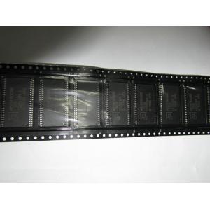
1 Megabit (128 K x 8-bit) CMOS 5.0 Volt-only, Uniform Sector Flash Memory
Add to Cart

Quick Detail:
8 Megabit (1 M x 8-Bit/512 K x 16-Bit) CMOS 5.0 Volt-only, Boot Sector Flash Memory
Description:
The Am29F800B is an 8 Mbit, 5.0 volt-only Flashmemory organized as 1,048,576 bytes or 524,288words. The device is offered in 44-pin SO and 48-pinTSOP packages. The word-wide data (x16) appears onDQ15–DQ0; the byte-wide (x8) data appears on DQ7–DQ0. This device is designed to be programmed in-system with the standard system 5.0 volt VCC supply.A 12.0 V VPP is not required for write or erase opera-tions. The device can also be programmed in standardEPROM programmers.This device is manufactured using AMD’s 0.35 µmprocess technology, and offers all the features and ben-efits of the Am29F800, which was manufactured using0.5 µm process technology.The standard device offers access times of 55, 70, 90,120, and 150 ns, allowing high speed microprocessorsto operate without wait states. To eliminate bus conten-tion the device has separate chip enable (CE#), writeenable (WE#) and output enable (OE#) controls.The device requires only a single 5.0 volt power sup-
ply for both read and write functions. Internally gener-ated and regulated voltages are provided for theprogram and erase operations.
The device is entirely command set compatible with theJEDEC single-power-supply Flash standard. Com-mands are written to the command register using stan-dard microprocessor write timings. Register contentsserve as input to an internal state-machine that con-
trols the erase and programming circuitry. Write cyclesalso internally latch addresses and data needed for theprogramming and erase operations. Reading data outof the device is similar to reading from other Flash orEPROM devices.Device programming occurs by executing the programcommand sequence. This initiates the EmbeddedProgram algorithm—an internal algorithm that auto-matically times the program pulse widths and verifiesproper cell margin.Device erasure occurs by executing the erase com-mand sequence. This initiates the Embedded Erasealgorithm—an internal algorithm that automatically
preprograms the array (if it is not already programmed)before executing the erase operation. During erase, thedevice automatically times the erase pulse widths andverifies proper cell margin. The host system can detect whether a program orerase operation is complete by observing the RY/BY#pin, or by reading the DQ7 (Data# Polling) and DQ6(toggle) status bits. After a program or erase cycle has
been completed, the device is ready to read array dataor accept another command. The sector erase architecture allows memory sectorsto be erased and reprogrammed without affecting thedata contents of other sectors. The device is fullyerased when shipped from the factory.Hardware data protection measures include a lowVCC detector that automatically inhibits write opera-tions during power transitions. The hardware sectorprotection feature disables both program and eraseoperations in any combination of the sectors of mem-ory. This can be achieved via programming equipment.The Erase Suspend feature enables the user to puterase on hold for any period of time to read data from,or program data to, any sector that is not selected forerasure. True background erase can thus be achieved.
The hardware RESET# pin terminates any operationin progress and resets the internal state machine toreading array data. The RESET# pin may be tied to thesystem reset circuitry. A system reset would thus alsoreset the device, enabling the system microprocessorto read the boot-up firmware from the Flash memory.The system can place the device into the standbymode. Power consumption is greatly reduced inthis mode.AMD’s Flash technology combines years of Flashmemory manufacturing experience to produce thehighest levels of quality, reliability and costeffectiveness. The device electrically erases allbits within a sector simultaneously viaFowler-Nordheim tunneling. The data isprogrammed using hot electron injection.
Applications:
— Pinout and software compatible with
single-power-supply flash
— Superior inadvertent write protection
n Data# Polling and Toggle Bits
— Provides a software method of detecting
program or erase cycle completion
Specifications:
Datasheets | AM29F800BB-70SE |
Standard Package | 960 |
Category | Integrated Circuits (ICs) |
Family | Memory |
Series | - |
Packaging | TAPE&REEl |
Format - Memory | FLASH |
Memory Type | FLASH |
Memory Size | 1M (512K x 16) |
Speed | 70ns |
Interface | Parallel |
Voltage - Supply | 4.5 V ~ 5.5 V |
Operating Temperature | -40°C ~ 85°C |
Package / Case | SOP44 |
Supplier Device Package | SOP44 |
Other Names | AM29F800BB-90SE |
Competitive Advantage:
Warranty :180days for all goods
Free shipping:Order over $600 win a free shipment fee:goods weight below 3Kg.
Mega Source Electronics stocks components ready to ship. Hard to find, obsolete and highly allocated integrated circuits and semiconductors are all can be found by us.
Mega Source Electronics has established a well-developed logistics system and global logistics network, which can guarantee our service very quick, convenient and efficient.
Tag:
AM29F800BB-70SE 8 Megabit (1 M x 8-Bit/512 K x 16-Bit) CMOS 5.0 Volt-only, Boot Sector Flash Memory


